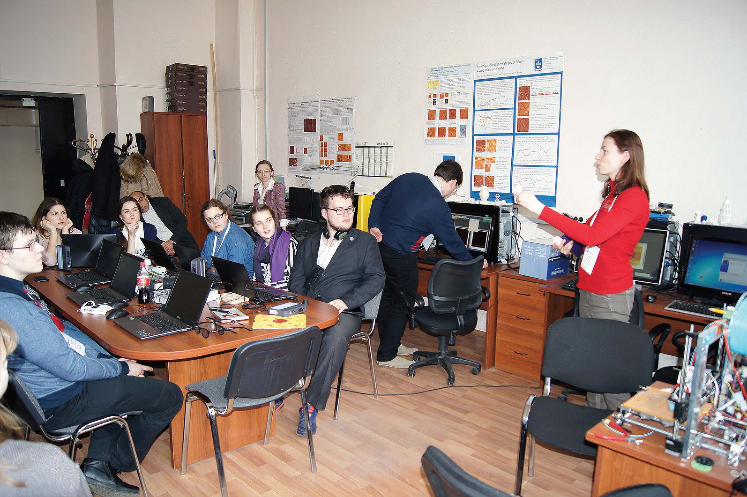
Olga Sinitsina is talking about nanotechnologies.
School graduates that have come to the admission committee of the physics faculty are usually asked why it is the MSU faculty of physics that they have chosen. The range of options is indeed very broad – it might be MIPT or MEPhI. A number of other higher educational institutions have also launched modern physics curricula. It often happens that we meet school graduates who are good both at physics and mathematics, which means they can also apply to such MSU faculties as those of mechanics and mathematics, and of computational mathematics and cybernetics. Among the reasons that make people come to the faculty of physics, one can hear, for example, “I’ve listened to an interesting lecture on biophysics” or “we were shown fascinating experiments with the laser”, and in recent years something like – “I’ve done some practical work at the physics faculty” or “I’ve attended classes on the digital modelling of physical processes”.
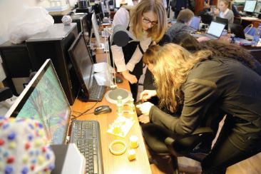
The students of the “Nanotechnologies” center are preparing their projects for the contest.
However, the classes attended at TSMIT (ЦМИТ) – the “Nanotechnologies” youth innovative creativity center of the MSU faculty of physics are probably the most attractive ones for school pupils, mainly because here they develop the skills necessary for using the most modern equipment: 3D printers, 3D scanners, machining centers with digital software, scanning probe microscopes.
In actual fact, the latter were created with the participation of the MSU physics faculty, and a few more words should be said in this connection. The 1986 Nobel Prize in Physics was given to G. Binnig and H. Rohrer – for creating the first scanning probe microscope (or scanning tunneling microscope). This prize was awarded for a new device, not a law or discovery. In the English version of the press release it is formulated as follows: “for their design of the scanning tunneling microscope”. In other words, one could say that this physics prize was awarded for an engineering design. Yes, that’s right. Many of the theoretical and practical aspects had been known long before: the tunneling effect, sharp atomic force microscope probes, exact nanometer measurements. But the key point was missing – a microscope demonstrating the atomic lattice on the surface of a substance. This Nobel Prize combines a profound understanding of physics and a talent for engineering – the qualities that turned out to be necessary for creating a new and unique device to observe atoms and molecules on the surface of materials using the metallic needle and the tunneling effect.
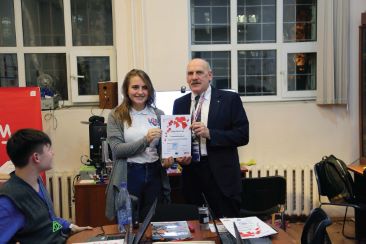
MSU Prof. I.V. Iaminsky is awarding the winners of the “Nanotechnologies” center’s contest winners.
One can easily claim that the year 1986 witnessed a new phenomenon, meaning that extremely sophisticated devices were designed by people were at the same time scientists, physicists and engineers. In this case the traditional division into scientists and engineers is neglected, and our work becomes more effective in many ways. Similarly, the first scanning tunneling microscope was devised in Russia by the research group headed by Prof. V.I. Panov, at the physics faculty of MSU. A brilliant knowledge of physics and a talent for engineering lead to this remarkable achievement.
The creation of the tunneling microscope reflected a very important idea – that outstanding results can be expected every time physics and engineering go together. It is in this direction that young talented budding physicists acquire practical skills in TSMIT at the physics faculty. An important role is played by learning to use electronic modelling computer programming systems: SolidWorks, SprutCam, Compass. Handling this software with skill gives the opportunity to make electronic models of components or entire devices. A model allows us to test efficiency, optimize the construction and exterior design, analyze mechanical strain under pressure, define resonance frequencies. The pupils are thus doing many of the things that help them to get rid of the disadvantages in a real device. It should be mentioned that the people attending TSMIT do not only make electronic models, but can also begin making the devices themselves, starting with the third session. They use the 3D printer to produce parts from plastic. There is a compact machining center for working with wood or metal.
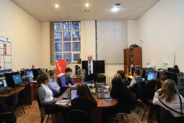
Prof. I.V. Iaminsky is holding a class on 3D printers, 3D microscopes and 3D production technologies in the “Nanotechnologies” center.
The basic theme of all the classes held at TSMIT is bringing to life the fastest and easiest pattern of turning a physical idea into a ready product of engineering. If the curriculum has been covered, the devices produced by the pupils can be shown to their friends and acquaintances in wooden, plastic or metallic form as a realization of their creative ideas.
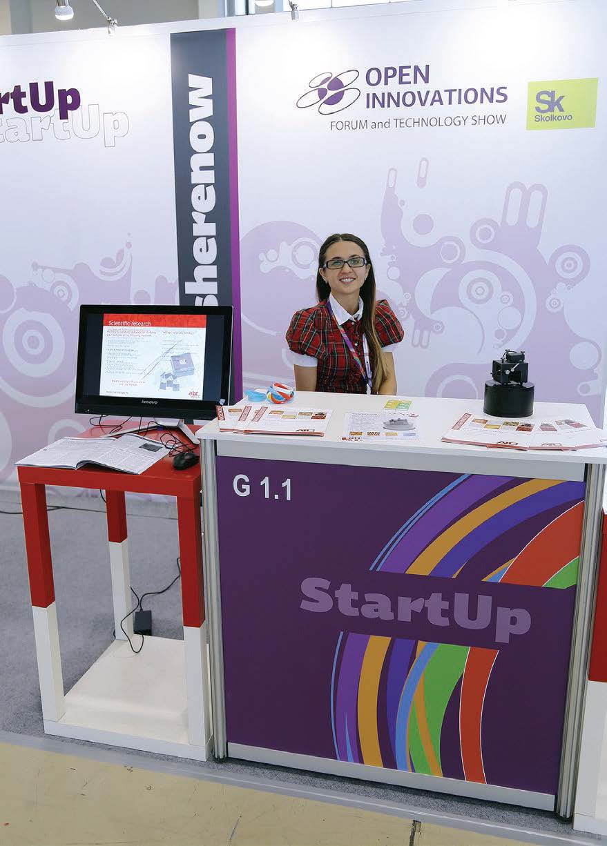
Assel Akhmetova at the Open Innovations exhibition. The “Nanotechnologies” center display board, October 2015.
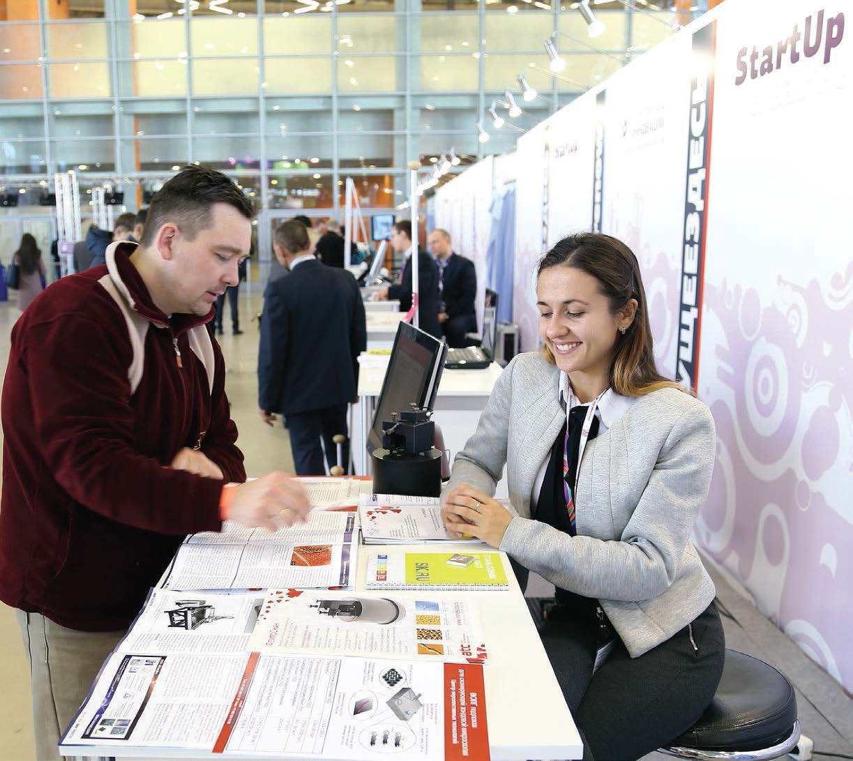
Registering new participants of the “Nanotechnologies” center at the Open Innovations exhibition, October 2015
The “Nanotechnologies” center currently holds classes on the following subjects: scanning probe microscopy (SPM), 3D modelling on the basis of the Solid Works system of automatic engineering; an introduction into machining using digital machining centers; the 3D printer; the 3D scanner.
For further information see the TSMIT website – www.startinnovation.com